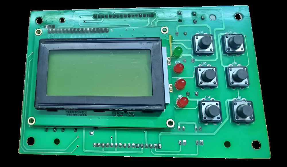
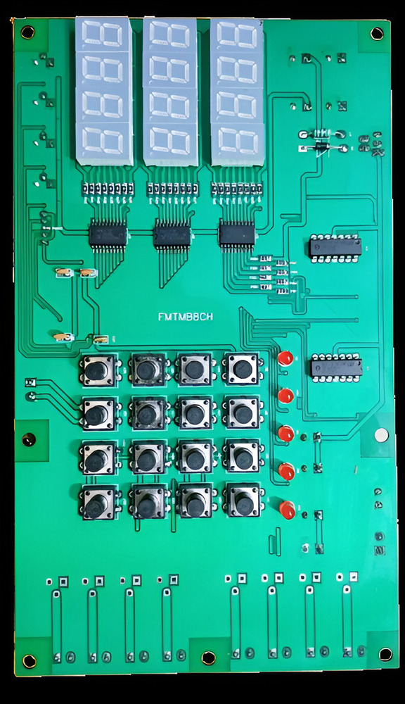
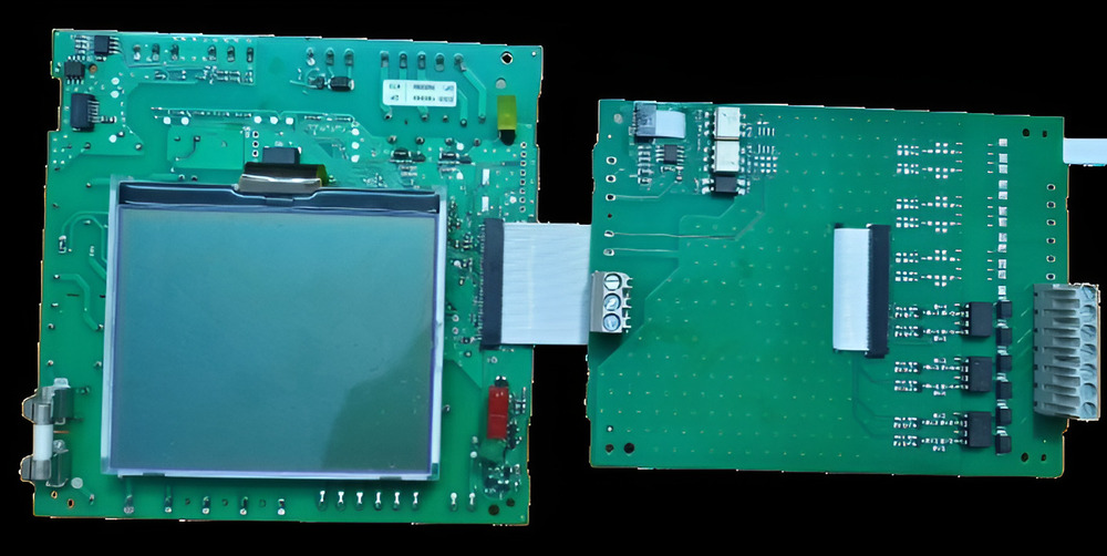
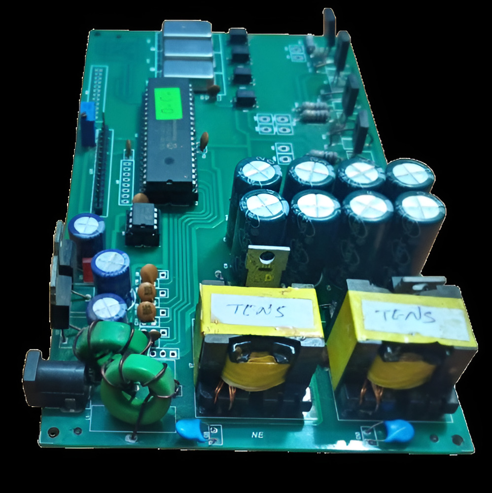
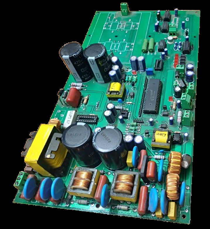
About Inverter PCB Design
We are having more than 20 years of design experience and are specialize in all kind of Electronics and Embedded circuits designs in Microcontroller, Analog and Digital circuits, Power Systems, AHF Designs, SVG Designs, single Phase and Three Phase UPS and Inverters design, APFC Relays, SCR Switching Boards, IGBT Switching Boards, Motor Control Boards, battery-powered handheld devices, motor drivers and controllers, power systems, boards etc. Our expertise is in electronics circuit design services with a schematic design to final product. This includes selecting relevant electronic components based on the product requirements already present in the product requirements document. Additionally, we elaborate circuit design with actual electronic connections based on functional diagrams.
We do development from concept to final product.
Precision Engineering for Reliable Inverter PerformanceOur inverter PCBs are engineered with tight control over trace width, hole size, and copper thickness, ensuring optimal electrical characteristics. The boards can be tailored for specific operating voltages, frequencies, and applications. Advanced testing procedures guarantee each unit's reliability, making them a sound choice for demanding inverter circuits.
Comprehensive Material and Finish OptionsEach board is constructed on FR4, a flame-retardant epoxy laminate for enhanced durability and safety. The HASL surface finish and green solder mask offer robust protection, while the white silkscreen ensures clear component marking. You can customize key parameters, including board dimensions and number of layers, to meet your precise requirements.
Strict Quality and Safety ComplianceAll inverter PCBs are RoHS compliant and 100% electrically tested for guaranteed safety and functionality. Impedance control is available upon request, catering to specialized applications. Antistatic packaging ensures that the boards arrive ready for accurate and safe integration into your assembly process.
FAQ's of Inverter PCB Design:
Q: What is the minimum trace width available for this inverter PCB design?
A: The minimum trace width for our inverter PCB design is 0.2 mm, allowing for compact and precise circuit layouts suitable for modern inverter applications.
Q: How do you ensure the quality and safety of these inverter PCBs?
A: Every inverter PCB is 100% electrically tested before delivery. The boards are also RoHS compliant, and are packaged in antistatic materials to maintain safety and performance standards throughout the supply chain.
Q: Where can these inverter PCBs be used and what are their main benefits?
A: These PCBs are designed specifically for inverter circuits in various electronic devices. The main benefits include high reliability, precise customization, compatibility with both SMD and through-hole mounting, and robust electrical and thermal performance.
Q: What is the manufacturing process for these inverter PCBs?
A: We use premium FR4 material, applying a HASL finish, green solder mask, and white silkscreen. Each board is fabricated with strict adherence to your sizing, layer, and component requirements, followed by full electrical testing prior to antistatic packaging.
Q: When is impedance control necessary for inverter PCB projects?
A: Impedance control is recommended if your inverter application is sensitive to signal integrity, particularly in cases involving high-speed switching or specific analog/digital requirements. This feature is available upon request.
Q: How can I customize the size and other specifications of the PCB?
A: You can specify the size, number of layers, mounting type, and other parameters when placing your order. Our team will work with you to ensure your design and technical requirements are fully met.
Q: What is the temperature and voltage range supported by these inverter PCBs?
A: These PCBs are suitable for operations between -40C to +85C and can handle operating voltages up to 400V, making them well-suited for a wide range of inverter applications.


 Send Inquiry


